
DUV workarounds strain Chinese chip margins
Analysts say multiple exposure techniques allow production without EUV tools, but yield losses and material costs are eroding profit potential for firms like SMIC and CXMT.
By Joseph Jenkins ·
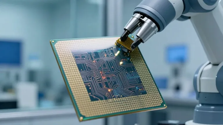
Chinese chip manufacturers are absorbing rising production costs to bypass the ban on extreme ultraviolet lithography, according to new analysis from Morgan Stanley. The bank estimates that domestic memory producer CXMT currently generates roughly one-third the bits per wafer compared to Western competitors. This efficiency gap stems from the reliance on deep ultraviolet equipment, which requires multiple passes to achieve densities that EUV tools print in a single exposure.
Morgan Stanley’s June report identified lithography access as a hard ceiling for China’s memory sector. Despite these constraints, the firm projects CXMT will increase its share of global DRAM bit supply from 14% in 2026 to 16% in 2028. The bank attributes this growth to the addition of new greenfield capacity rather than improvements in yield rates. The same report suggests China’s self-sufficiency in AI chips will climb from 42% in 2025 to 70% by 2030, though a persistent gap remains in high-bandwidth memory and advanced software.
Industry experts note that the cost of this workaround strategy is escalating. Chris Mack, co-founder and CTO of Fractilia, stated that industry wisdom holds three exposures on a 193 immersion tool cost about the same as one EUV pass. At four masks, however, the older technology becomes the more expensive option. Each additional pattern requires precise alignment with previous layers, leading to accumulated overlay errors and greater process variation.
Designers often compensate for these errors by adding space around features, which enlarges the die size. This reduces the number of usable dies per wafer, a costly outcome when wafers price in the tens of thousands of dollars. Mack emphasized that manufacturers sell individual dies, not raw wafers, meaning lower yield rates directly impact revenue. He added that while SMIC’s N+3 process represents progress, it remains significantly less scaled than the established 5nm processes offered by Samsung and TSMC.
The multiple patterning technique allows companies to split complex designs into simpler patterns, building up the intended layer step by step. This approach has enabled SMIC to produce the Kirin 9000S processor for Huawei’s Mate 60 Pro using a second-generation 7nm-class process without EUV. Recent analysis of the Kirin 9030 indicates SMIC has moved its DUV-based process closer to the density associated with 5nm manufacturing, though it still trails the leading nodes from TSMC and Samsung.
Memory production offers a clearer view of the efficiency gap. Micron developed its 1-alpha DRAM without EUV, using multiple patterning and tight process control. Mack noted that Micron pushed 193 immersion technology farther than other memory makers. Morgan Stanley considers CXMT’s planned move to 1-alpha DRAM for HBM3e achievable without EUV. However, Micron eventually turned to EUV for its 1-gamma DRAM, which delivers more than 30% greater bit density per wafer than the previous generation.
Advanced packaging may offer a partial solution in the long term. Douglas Fuller, a researcher at Copenhagen Business School, expects this technology to allow firms to use DUV for the latest DRAM generations by the end of the decade. Mack cautioned that China could make further progress if it had the full 193 immersion ecosystem and designed products specifically around it. He stressed that memory is much easier to manufacture than logic chips, noting that EUV has its own drawbacks, including stochastic effects that require higher exposure doses and greater costs.
Mack said he would be hard pressed to believe a 3nm or 2nm node could be economically viable without EUV. Chinese chipmakers are not expected to stall, however. They can continue pushing DUV while accepting larger dies, poorer yields, and longer manufacturing times. They can also add capacity to offset these losses. The industry expects this trade-off between cost and capability to define the competitive landscape for Chinese silicon production in the coming years.
Source: Tom's Hardware